Back Flip xip Catalan Flip-Chip-Montage German Flip chip Spanish تراشه برگردان Persian Puce retournée French Flip Chip NB Flip chip Russian Flip chip Swedish Flip chip Ukrainian 覆晶技術 Chinese


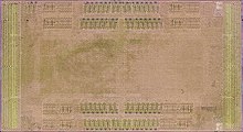
Flip chip, also known as controlled collapse chip connection or its abbreviation, C4,[1] is a method for interconnecting dies such as semiconductor devices, IC chips, integrated passive devices and microelectromechanical systems (MEMS), to external circuitry with solder bumps that have been deposited onto the chip pads. The technique was developed by General Electric's Light Military Electronics Department, Utica, New York.[2] The solder bumps are deposited on the chip pads on the top side of the wafer during the final wafer processing step. In order to mount the chip to external circuitry (e.g., a circuit board or another chip or wafer), it is flipped over so that its top side faces down, and aligned so that its pads align with matching pads on the external circuit, and then the solder is reflowed to complete the interconnect. This is in contrast to wire bonding, in which the chip is mounted upright and fine wires are welded onto the chip pads and lead frame contacts to interconnect the chip pads to external circuitry.[3]
- ^ E. J. Rymaszewski, J. L. Walsh, and G. W. Leehan, "Semiconductor Logic Technology in IBM", IBM Journal of Research and Development, 25, no. 5 (September 1981): 605.
- ^ Filter Center, Aviation Week & Space Technology, September 23, 1963, v. 79, no. 13, p. 96.
- ^ Peter Elenius and Lee Levine, Chip Scale Review. "Comparing Flip-Chip and Wire-Bond Interconnection Technologies". July/August 2000. Retrieved July 30, 2015.
© MMXXIII Rich X Search. We shall prevail. All rights reserved. Rich X Search