Back معمارية هارفارد Arabic Харвардска архитектура Bulgarian Arquitectura Harvard Catalan Harvardská architektura Czech Harvard-Architektur German Αρχιτεκτονική Χάρβαρντ Greek Arquitectura Harvard Spanish Harvardi arhitektuur Estonian Harvard arkitektura Basque معماری هاروارد Persian
This article needs additional citations for verification. (March 2011) |

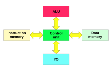
The Harvard architecture is a computer architecture with separate storage and signal pathways for instructions and data. It is often contrasted with the von Neumann architecture, where program instructions and data share the same memory and pathways. This architecture is often used in real-time processing or low-power applications.[1][2]
The term is often stated as having originated from the Harvard Mark I relay-based computer, which stored instructions on punched tape (24 bits wide) and data in electro-mechanical counters. These early machines had data storage entirely contained within the central processing unit, and provided no access to the instruction storage as data. Programs needed to be loaded by an operator; the processor could not initialize itself. However, in the only peer-reviewed published paper on the topic – The Myth of the Harvard Architecture published in the IEEE Annals of the History of Computing[3] – the author demonstrates that:
- 'The term "Harvard architecture" was coined decades later, in the context of microcontroller design' and only 'retrospectively applied to the Harvard machines and subsequently applied to RISC microprocessors with separated caches';
- 'The so-called "Harvard" and "von Neumann" architectures are often portrayed as a dichotomy, but the various devices labeled as the former have far more in common with the latter than they do with each other';
- 'In short [the Harvard architecture] isn't an architecture and didn't derive from work at Harvard'.
Modern processors appear to the user to be systems with von Neumann architectures, with the program code stored in the same main memory as the data. For performance reasons, internally and largely invisible to the user, most designs have separate processor caches for the instructions and data, with separate pathways into the processor for each. This is one form of what is known as the modified Harvard architecture.
Harvard architecture is historically, and traditionally, split into two address spaces, but having three, i.e. two extra (and all accessed in each cycle) is also done,[4] while rare.
- ^ Kong, J. H.; Ang, L. M.; Seng, K. P. (2010). "Minimal Instruction Set AES Processor using Harvard Architecture". 2010 3rd International Conference on Computer Science and Information Technology. Vol. 9. pp. 65–69. doi:10.1109/ICCSIT.2010.5564522. ISBN 978-1-4244-5537-9.
- ^ Venkatesan, Chandran; Sulthana, M. Thabsera; Sumithra, M. G.; Suriya, M. (2019). "Design of a 16-Bit Harvard Structure RISC Processor in Cadence 45nm Technology". 2019 5th International Conference on Advanced Computing & Communication Systems (ICACCS). pp. 173–178. doi:10.1109/ICACCS.2019.8728479. ISBN 978-1-5386-9531-9.
- ^ Pawson, Richard (30 September 2022). "The Myth of the Harvard Architecture". IEEE Annals of the History of Computing. 44 (3): 59–69. doi:10.1109/MAHC.2022.3175612. S2CID 252018052.
- ^ "Kalimba DSP: User guide" (PDF). July 2006. p. 18. Retrieved 2022-09-23.
this is a three-bank Harvard architecture.
© MMXXIII Rich X Search. We shall prevail. All rights reserved. Rich X Search