Back Kikuchi-Linien German 菊池像 Japanese Linha de Kikuchi Portuguese Кикучи-линия Russian Đường Kikuchi Vietnamese 菊池線 (物理) Chinese

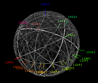
Kikuchi lines are patterns of electrons formed by scattering. They pair up to form bands in electron diffraction from single crystal specimens, there to serve as "roads in orientation-space" for microscopists uncertain of what they are looking at. In transmission electron microscopes, they are easily seen in diffraction from regions of the specimen thick enough for multiple scattering.[1] Unlike diffraction spots, which blink on and off as one tilts the crystal, Kikuchi bands mark orientation space with well-defined intersections (called zones or poles) as well as paths connecting one intersection to the next.
Experimental and theoretical maps of Kikuchi band geometry, as well as their direct-space analogs e.g. bend contours, electron channeling patterns, and fringe visibility maps are increasingly useful tools in electron microscopy of crystalline and nanocrystalline materials.[2] Because each Kikuchi line is associated with Bragg diffraction from one side of a single set of lattice planes, these lines can be labeled with the same Miller or reciprocal-lattice indices that are used to identify individual diffraction spots. Kikuchi band intersections, or zones, on the other hand are indexed with direct-lattice indices i.e. indices which represent integer multiples of the lattice basis vectors a, b and c.
Kikuchi lines are formed in diffraction patterns by diffusely scattered electrons, e.g. as a result of thermal atom vibrations.[3] The main features of their geometry can be deduced from a simple elastic mechanism proposed in 1928 by Seishi Kikuchi,[4] although the dynamical theory of diffuse inelastic scattering is needed to understand them quantitatively.[5]
In x-ray scattering, these lines are referred to as Kossel lines[6] (named after Walther Kossel).
- ^ David B. Williams; C. Barry Carter (1996). Transmission electron microscopy: A textbook for materials science. Plenum Press, NY. ISBN 978-0-306-45324-3.
- ^ K. Saruwatari; J. Akai; Y. Fukumori; N. Ozaki; H. Nagasawa; T. Kogure (2008). "Crystal orientation analyses of biominerals using Kikuchi patterns in TEM". J. Mineral. Petrol. Sci. 103: 16–22. doi:10.2465/jmps.070611.
- ^ Earl J. Kirkland (1998). Advanced computing in electron microscopy. Plenum Press, NY. p. 151. ISBN 978-0-306-45936-8.
- ^ S. Kikuchi (1928). "Diffraction of Cathode Rays by Mica". Japanese Journal of Physics. 5 (3061): 83–96. Bibcode:1928Natur.121.1019N. doi:10.1038/1211019a0.
- ^ P. Hirsch; A. Howie; R. Nicholson; D. W. Pashley; M. J. Whelan (1977). Electron microscopy of thin crystals. Butterworths/Krieger, London/Malabar FL. ISBN 978-0-88275-376-8.
- ^ R. W. James (1982). "Chapter VIII". The Optical Principles of the Diffraction of X-Rays'. Ox Bow Press, Woodbridge, Connecticut. ISBN 978-0-918024-23-7.
© MMXXIII Rich X Search. We shall prevail. All rights reserved. Rich X Search